
I have worked with a CNC milling machine for my graduation project, at that time my instructor told me about using the CNC machine to produce a PCB since that I was curious about it. In this day I have learned about the PCB milling machine.
The day started by the design of the programmer. I have not designed it instead, I have downloaded it as a png picture. This website fabmodules is where the picture is converted to .rml format.
After the picture has been converter to the required format, I have started to set up the machine which is the SRM-20 machine.
The following images show the process of setting up the machine and preparing the spindle.


FR1 paper is used to produce the PCB, for the programmer one side paper is used, but for more complicated designs double side paper could be used. There are other types of paper like the FR4, but it is not recommended. When I was preparing the paper, I have hold it in the wrong way. My fingerprint can be seen in the following image, this may cause a short circuit if any design is produced over it.
The following photo also shows a number of milling bits. For the traces 1/64" bit will be used whereas 1/32" bit for the cover both are two flutes with the spindle diameter of 3.175mm. The cutting part of the bit must not too tall so that it does not break during the operation especially the traces bit.

The following image shows a rigid box of foam, this box is placed inside the machine because the bit can not go down in the z-axis and reach the paper. The following pictures show the process of placing the paper on the foam with a double face tape. During this process, I have checked several time for any bubbles. These bubbles will cause the surface to be uneven and may cause the bit to break.

Next step was to place the milling bit, this process is very sensitive, so the first thing to do was placing a sheet of cartoon over the FR1 paper to protect the bit if it falls down during the installation process. I have used two fingers also as shown in the following image to make sure the bit does not fall. I have fixed bit so that at least 20% of the spindle is visible for the purpose of setting up the zero z-axis.

After setting up the SRM-20, I have downloaded the software starting from this link, I have opened an account on roland support to be able to download the software.
Now the machine is connected to the computer. Before doing anything or starting any operation, the origin should be set. There are two coordinates, user and machine coordinated. User coordinate system should be zero in all directions then the milling operation can be started.
The traces image with a 1000dpi quality can be found here and the cut image with the same quality can be found here
Last step is to remove the programmer from the FR1 paper, this can be done using a screw driver. The programmer must be removed easily otherwise start the operation again with a deeper z-axis. Fortunately the programmer is removed from the first time.

The first programmer had a short circuit, the problem is that the picture of the design is 600dpi so to solve this problem I have downloaded another picture for the same design, but with higher dpi. It was 1000 dpi.
ِAfter I have produced the PCB, I have started soldering the components. All the components are surface mounted which means that the component will not fit inside a hole, instead it will soldered on the PCB surface directly.
To start soldering, frist thing I did is preparing the soldering station. I have a solder station which needs a 110V input so I needed a transformer to covert the 220v output to the needed 110v.

Next, I have prepared the parts:
It not my first time to solder parts, actually I have soldered through hole components before, but this is my first time to solder surface mounted devices (SMD). The following image shows SMD soldering procedure.
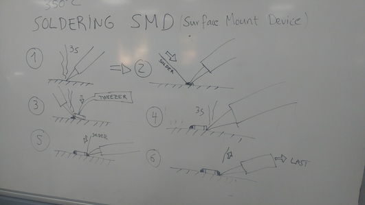
One of the major differences I have found between through hole and SMD is that the component legs in the SMD is very small. I tired to use the magnifying glasses, but I found it difficult to solder so I relied on my naked eyes.

After I have soldered the components, I have tested the functionality by inspecting a short circuit and if the circuit is closed or not using a multimeter. The multimeter will make a beep sound if the circuit is closed.
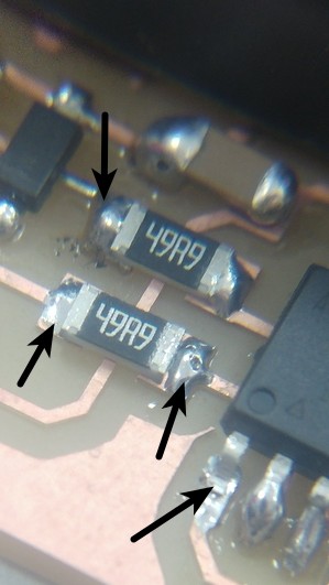
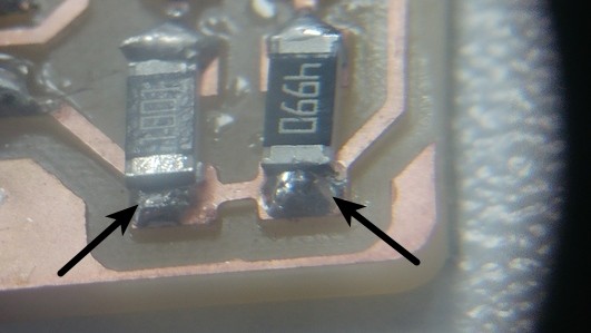
I had four soldering defects, all in which the components were not soldered properly. The following images shows the defects.
500 ohm and the second leg of the micro controller were not soldered properly.
The diode and the 50 ohm resistor were also not soldered properly.
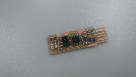
Another check I have did is to plug the usb to a USB port, the Red LED was illuminated.
Now that my programmer is ready to be programmed,
I have installed the toolchain and the firmware using the following steps. First run the command sudo apt install avrdude gcc-avr avr-libc make, then I have downloaded the firmware from this link, after that, I have opened the firmware directory using the command cd "directory" then I have executed the following command make to make the .hex file which will be uploaded to the miro controller.
To upload the .hex file, I will use atmelice so I have opened the Makefile using atom and changed the PROGRAMMER to atmelice then I have executed the following commands make flash, make fuses, make rstdisbl, make rstdisbl.
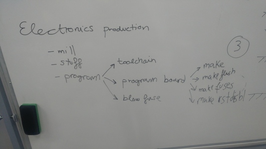
During this process, I have faced a problem which states that there is a problem with the connection, I have looked for a solution and found it in this link. The solution was to change the PROGRAMMER to atmelice_isp instead of atmelice.
My board is now a programmer, to the functionality of it, my classmates boards have used it to program their boards. They have followed the same procedure, but the PROGRAMMER was changed from atmelice_isp to usbtiny.
The following images show the procedure of making the connector cable so that my programmer could be used to program other boards.
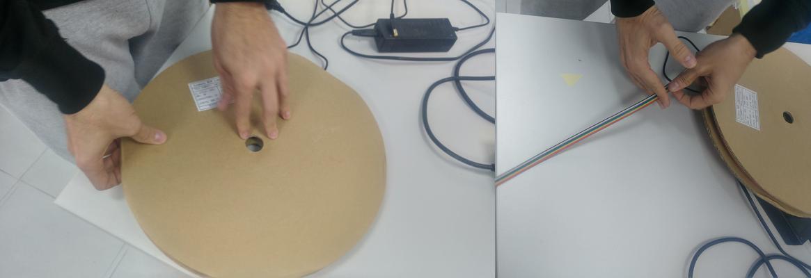
One end of the cable must be twisted then inserted as shown in the following below.

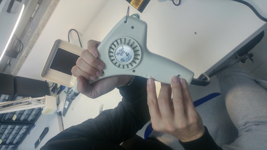
A heat gun is used to remove the soldered components, this gun heats air up to 400 degreed celius. The component should be holded by a tweezers during the process. The heat gun should be switched to cold air before shutting it down so that all the heat inside the gun is removed.
The programmer was a pre-designed circuit, but now it is time to design and produce my own circuit. The PCB has a very simple design, a LED controlled by a button.
The components are:
Kokopelli is the software to design a PCB using python. I have not designed the circuit from scratch because it will take me a lot of time, instead I have modified a previous design.
I have downloaded the software from this link, and then used the command make fab to compile all the files and then opened the bin folder by the command cd bin and finally started the software using the command ./kokopelli -r
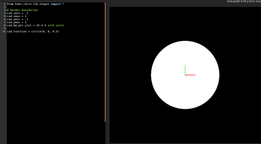
The source code of the original design can be found in this link.
BU1 = button_6mm('BU1');
pcb = BU1.add(pcb,XTAL1.x+0.02,J1.y+0.1,z,90);
pcb = wire(pcb,w,IC1.pad[5],BU1.pad[4])
pcb = wire(pcb,w,J1.pad[6],BU1.pad[2])

LED1 = LED_1206('LED');
pcb = LED1.add(pcb,IC1.x+0.3,IC1.pad[10].y,z,180)

R2 = R_1206('R2');
pcb = R2.add(pcb, LED1.x+0.06,LED1.y-0.2,z,90)
pcb = wire(pcb,w,IC1.pad[10],LED1.pad[2])
pcb = wire(pcb,w,LED1.pad[1],R2.pad[2])
pcb = wire(pcb,w,J1.pad[2],R2.pad[1])
I have added my parts which they are the LED, 100ohm resistor and the button as shown inside the square in the following image.
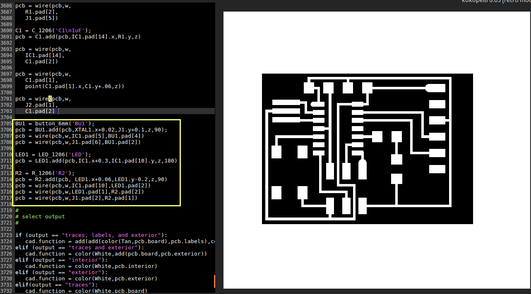
The idea is to switch on the LED when the button is pressed. The LED is connected to the 5v trace and the button is connected to GND trace.
The final design is shown in the following image

The best image quality is 40 pixels/mm which corresponds to 1000dpi.
The following images are the original size of the traces and the cut.
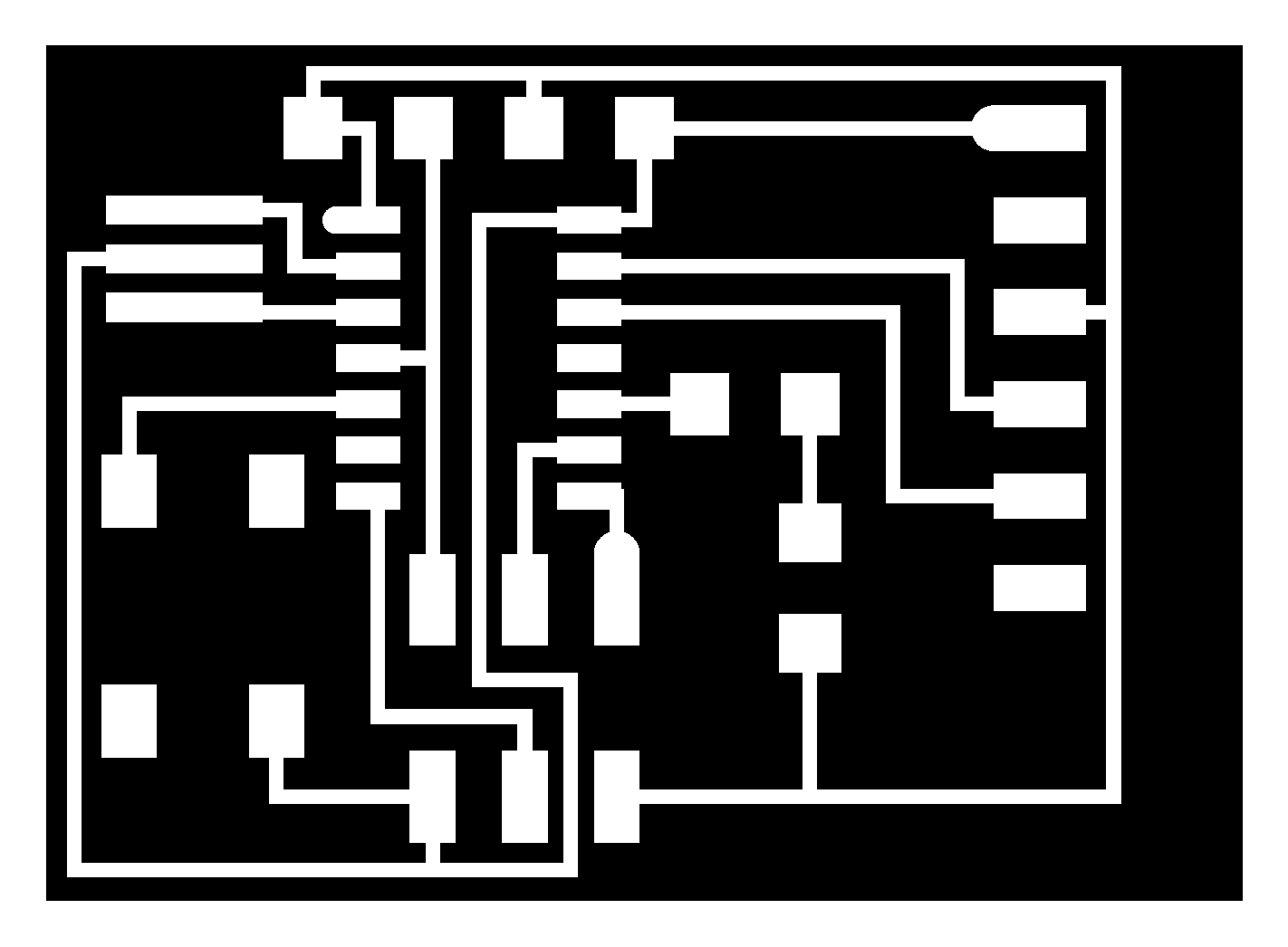

Now that the design is ready, I have produced the PCB using the SRM-20 machine and started soldering the components. After I have finished soldering the micro controller I have found that it is not soldered in the correct orientation ! I had to desolder it using the heat gun and remove the solder by the wick then solder it again.
Programming in C is explained in the programming documentation
My board is ready to be programmed, the program is written in C and the programmer which I milled previously will be used as the interface between my computer and the board.
The code is shown bellow
#define F_CPU 1000000UL
#include <avr/io.h>
#include <util/delay.h>

int main (void)
{

 DDRA = 0b00001000; // set PA3 as output in DDRB.
 DDRB = 0b00000000; // set PB2 as input in DDRB.
 PORTB = 0b00000100; // activate pull up resistor.

 while(1) {

   if(PINB == 0b00000000){ // if the button is pressed the micro controller will read 0 on PB2

     PORTA = 0b00000000; // Write 0 on PA3 to switch on the LED
   }else{
     PORTA = 0b00001000; // Write 1 on PA3 to switch off the plugged
   }
}
}
To upload the code I have connected the board with the programmer and plugged the programmer into a USB port then I have executed the commands make flash then make program.
The LED now will be switched on when the button is pressed.
I have made a slight modification to the make file to be able to use make program and make flash for a specific file

Now I can use the makefile for any file I want instead of the predefined filename by adding filename = your file name after make program and make flash like this make program filename = program.c
Pull up resistor is a piece of hardware used to ensure that the inputs settle at the logical level (0 or 1). Just because the input pin is not connected to anything, the pin reads a constant state like 0. For example, the previous project is about controlling an LED when the button is pressed. If I have not used the internal pull up resistor, the LED will be switched on and off several times without me pressing the button !
Pull up resistor is basically a 5 volt source connected in series with a resistor. The resistor is connected to the input pin and the switch (in my case the button). The button is connected to the ground.
When the pull up resistor is initiated, the pin will read 1 (5v). If the button is pressed the resistor will be connected with the ground and the pin will read 0.
A major problem with buttons is the switch bounce, which appears when pressing the button (changing the state). Button bounce is a design problem and it is effect depends on the quality of the switch. When a button is pressed, the state will be changed from 0 to 1 or from 1 to 0, actually this change is not happening instantly, the state will be changed several times before it becomes stable at the new state. The microcontroller will think that the button has been pressed several times, but we have pressed it only once !
I have used the oscilloscope to view the bouncing effect of the button I used in the board.
The following picture shows the bouncing effect. The state changes three times when the button is pressed, I have used a very good quality button !
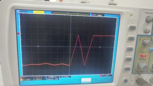
To eliminate the bouncing effect, I have used a 10 microfarads capacitor and the result is showed in the following picture.
