Electronics production session was started off by Mr. Fransisco guiding us how to install the miller cutter machine (SRM-20) which we will be using it later to print our circuit boards.
After we had removed the machine from her package, we removed the cartoon pieces that has been placed within the machine to protect her parts during the shipment process. Then, we started installing the machine.
Firstly, we installed the head that will hold the milling bits.

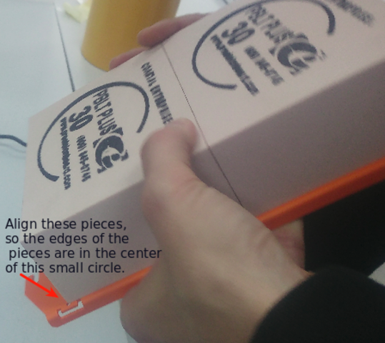
Then we started preparing the base where the FR1 papers will be put down to be milled later for making electronic circuit boards. It is so important to align the base correctly.
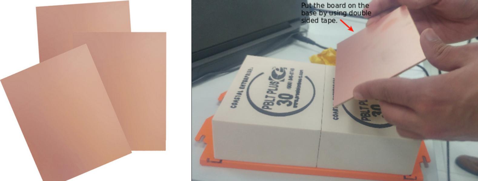
after we finished the base settings, we put the FR1 paper down on the base by using double sided tape.Also, we had made sure that the FR1 papers are aligned with the base in order to get an accurate circuit boards. Mr. Fransisco told us that we can buy the FR1 Paper by accessing inventables.com. Mr. Fransisco told us that the FR1 papers could be one sided or double sided; the double sided papers are used if we want to print a circuit board with two layers.
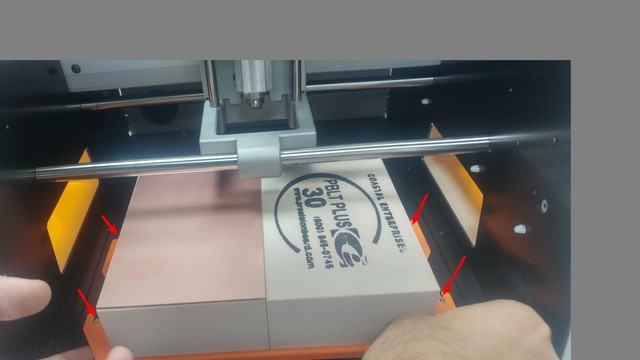
While we inserting the base within the machine we aligned it with four holes located in the machine. and fix the base using screws.
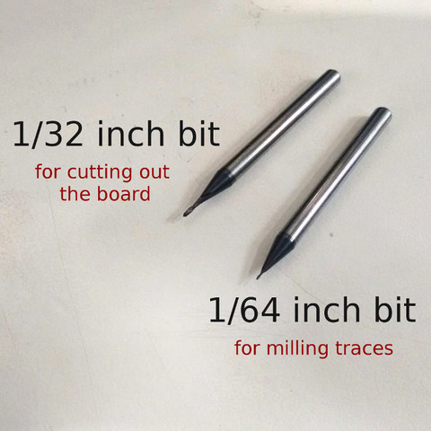
Mr. Fransisco has told us that we will use the 1/64 milling bit for traces and the 1/32 milling bit for cutting the board. Then i ahve asked Mr. Fransisco what milling bit should I use for vias, and his answer was that I should use the 1/32 milling bit.
After the settings of the machine has been done, Mr. Fransisco started guiding us to use the machine for printing circuit boards. The steps we followed in order to git a functional circuit boards can be summarized as follow:
Once we finished the design of our circuit boards, we saved them with .png extension then we convert them to be with .rml extension by accessing fabmodules website.
we uploaded the first image (traces.png) which will be for traces.


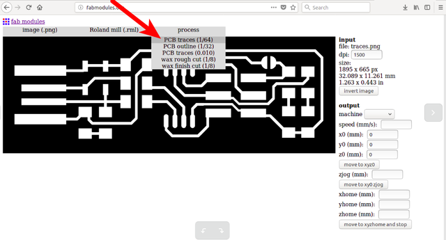
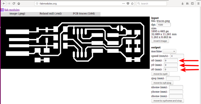
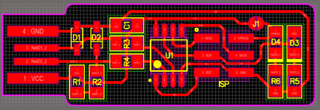
Because this the first time for us to print circuit boards and to test the machine, Mr. Fransisco asked us to download a pre-designed circuit board, it was for an ATtiny programmer. Also, we will use this circuit board to be our programmer during the pre-fab academy; it will be the interface between the computer and other circuit boards that need to be programmed.
Then I turned on the machine SRM-20 in order to print the board and we connected it with the computer through USB cable and we controlled it through the software.
First of all I have to insert the 1/64 milling bit because we make the traces at beginning. But before that I have to put a peace of cartoon on the base in order to protect the milling bit from breaking in case it fallen down. And I have to insert around 80% of the milling bit on the head of the machine.

Then I have to move the milling bit through the (x+,x-),(y+,y-) and (z+,z-) buttons and put it at the point that I am going to start milling from. Mr. Fransisco has told us that once we are going o move the milling bit in the z- we have to activate the steps x100 or x10 or x1 mm and deactivate the continue choice to avoid breaking the milling bit by hitting it on the base. and once the milling bit is 1mm far away from the FR1 paper we have then to untight the screw and down the milling bit by hand until it touch the FR1 paper then re-tightening the milling bit.
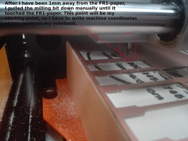
After doing this I have to write down on the notebooks the machine coordinate system points, to use them in case I need them. for example if the electricity outage is happened. and then going back to the user coordinate system and reset the x,y and z points. Then I started milling by press the cut button and uploading the .rml file.
After the machine had milled the traces and cut the board, I removed it out of the FR1 paper.

I have used the following components to solder on our programmer circuit board:
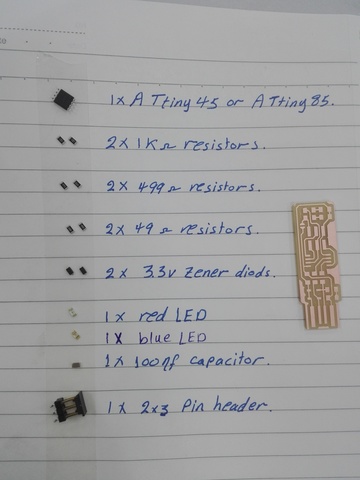
know I can start soldering the board. But before I started, Mr. Fransisco had told us about the precautions and the procedures for soldering surface mount components:
Soldering procedures:
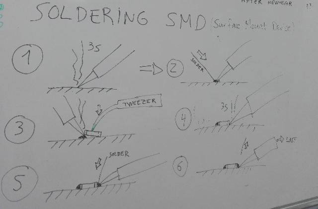
Actually, I have an experience in soldering for both through hole and surface mount devices SMD. So, I didn't face any problems during the soldering process and after finishing I tested the board and it was functional.
precautions:
After I finished soldering the components on the programmer circuit board I started programming it to use it later as an interface between the computer and the micro controller circuits. To program the board I followed the procedures on this link.
Mr. Fransisco asked us to think about a circuit using the ATtiny 44 micro-controller with one input and one output. After discussing we agreed to use push button as an input and LED as an output. And we started designing the circuit board by kokopelli software, which is an open-source tool for computer-aided design and manufacturing (CAD/CAM).
To run the sofware we wrote in the terminal the following commands:
make fabcd bin./kokopelli -rAfter running the software the following picture is appear.

The left side is where I wrote the code that will sketch the circuit board while the right side is where the circuit board is appear.
In order to design the circuit board I have copied the code text where all the components are defined from this link. Then I started writing my own code text for designing in define board section. The text for my circuit design was as follow:
# define board

w = .016
width = 1.1
height = .93
mask = .004
x = 1
y = 1
z = -.005
d = .06

pcb = PCB(x,y,width,height,mask)

IC1 = ATtiny44_SOICN('IC1\nt44')
pcb = IC1.add(pcb,x+.47,y+.59,z)

J1 = header_ISP('J1\nISP')
pcb = J1.add(pcb,IC1.x+.05,IC1.pad[7].y-.22,z,angle=90)

pcb = wire(pcb,w,IC1.pad[8],J1.pad[1])

pcb = wire(pcb,w,IC1.pad[9],J1.pad[3])

pcb = wire(pcb,w,IC1.pad[7],point(IC1.pad[7].x+.01,J1.y-.02,z),J1.pad[4])

pcb = wire(pcb,w,IC1.pad[4],J1.pad[5])

pcb = wire(pcb,w,IC1.pad[14],point(J1.x-.05,J1.y+.02,z),point(J1.x+.05,J1.pad[2].y-.08,z),J1.pad[6])

J2 = header_FTDI('J2 FTDI')
pcb = J2.add(pcb,x+width-.08,IC1.y-.0,z,angle=0)

pcb = wire(pcb,w,J1.pad[2],point(J2.x+.08,J2.pad[3].y,z),J2.pad[3])

pcb = wire(pcb,w,IC1.pad[13],point(IC1.pad[13].x+.35,J2.pad[4].y,z),J2.pad[4])

pcb = wire(pcb,w,IC1.pad[12],point(IC1.pad[12].x+.3,J2.pad[5].y,z),J2.pad[5])

XTAL1 = XTAL_EFOBM('XTAL1\n20 MHz')
pcb = XTAL1.add(pcb,IC1.pad[4].x-.2,IC1.pad[13].y+.008,z,angle=-90)

pcb = wire(pcb,w,IC1.pad[2],point(XTAL1.x+.12,XTAL1.pad[1].y,z),XTAL1.pad[1])

pcb = wire(pcb,w,J1.pad[6],point(J1.pad[6].x,J1.pad[6].y-.08,z),
point(XTAL1.x-.12,XTAL1.pad[2].y,z),XTAL1.pad[2])

pcb = wire(pcb,w,IC1.pad[3],XTAL1.pad[3])

R1 = R_1206('R1\n10k');
pcb = R1.add(pcb,IC1.pad[1].x,IC1.pad[1].y+.1,z)

pcb = wire(pcb,w,R1.pad[1],IC1.pad[1])

pcb = wire(pcb,w,J2.pad[3],point(J2.pad[3].x+.08,R1.y+.06,z),R1.pad[1])

pcb = wire(pcb,w,R1.pad[2],J1.pad[5])

C1 = C_1206('C1\n1uF');
pcb = C1.add(pcb,IC1.pad[14].x,R1.y,z)

pcb = wire(pcb,w,IC1.pad[14],C1.pad[2])

pcb = wire(pcb,w,C1.pad[1],point(C1.pad[1].x,C1.y+.06,z))

pcb = wire(pcb,w,J2.pad[1],C1.pad[2])

BU1 = button_6mm('BU1');
pcb = BU1.add(pcb,XTAL1.x+0.02,J1.y+0.1,z,90);
pcb = wire(pcb,w,IC1.pad[5],BU1.pad[4])
pcb = wire(pcb,w,J1.pad[6],BU1.pad[2])

LED1 = LED_1206('LED');
pcb = LED1.add(pcb,IC1.x+0.3,IC1.pad[10].y,z,180)

R2 = R_1206('R2');
pcb = R2.add(pcb, LED1.x+0.06,LED1.y-0.2,z,90)
pcb = wire(pcb,w,IC1.pad[10],LED1.pad[2])
pcb = wire(pcb,w,LED1.pad[1],R2.pad[2])
pcb = wire(pcb,w,J1.pad[2],R2.pad[1])
The following picture is the resulted circuit board of the above code:
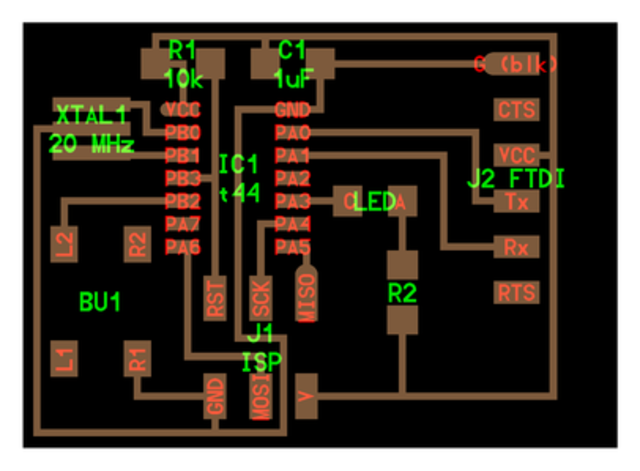
On PCBs, It's clear to see that R refers to resistors, D refers to diodes, C refers to capacitors and J refers to connectors. For more info about PCB markings we could access this link.
This is the board after finishing the soldering process.
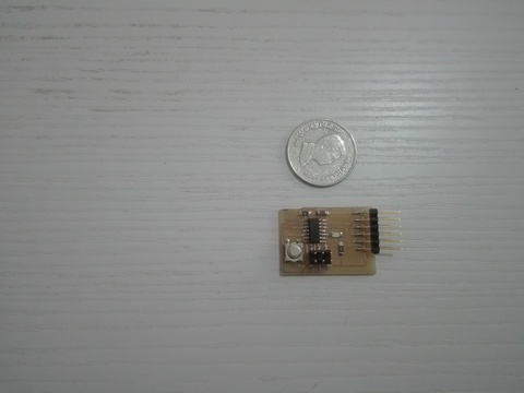
After I had finished soldering the board, I made a cable which will connect the programmer board with the microcontroller board in order to upload programs from the computer to the microcontroller circuit.

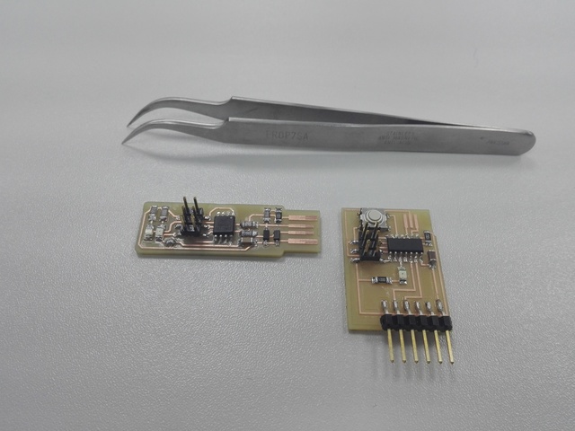
And finally, here is the microcontroller and the programmer boards.
